Nature paper reports making and moving large-scale hexagonal boron nitride
 Step by step, scientists are figuring out new ways to extend Moore’s Law. The latest reveals a path toward integrated circuits with two-dimensional transistors.
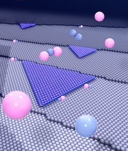
A Rice University scientist and his collaborators in Taiwan and China reported in Nature today that they have successfully grown atom-thick sheets of hexagonal boron nitride (hBN) as two-inch diameter crystals across a wafer.
Surprisingly, they achieved the long-sought goal of making perfectly ordered crystals of hBN, a wide band gap semiconductor, by taking advantage of disorder among the meandering steps on a copper substrate. The random steps keep the hBN in line.
Brown School of Engineering materials theorist Boris Yakobson is co-lead scientist on the study with Lain-Jong (Lance) Li of the Taiwan Semiconductor Manufacturing Co. (TSMC) and his team. Yakobson and Chih-Piao Chuu of TSMC performed theoretical analysis and first principles calculations to unravel the mechanisms of what their co-authors saw in experiments.
– See more at Rice News


