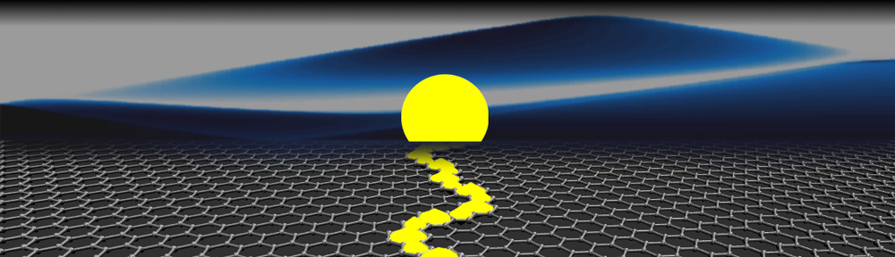
The January 21 issue of Adv. Funct. Mater. features on its back cover work on graphene grain boundaries
 The image shows a simulated grain boundary stitching two graphene domains tilted at a 28° angle exhibits a well-defined sinuous shape, which is revealed to be energetically preferred. Such sinuous grain boundary, appeared to be a curved river on land, are highlighted by B. I. Yakobson and co-workers on page 367 as a new channel to explore novel electronic behavior in graphene and to reach the as yet unexplored flatlands of two-dimensional materials.
