Rice lab peers inside 2D crystal synthesis

Simulations could help molecular engineers enhance creation of semiconducting nanomaterials

Scientific studies describing the most basic processes often have the greatest impact in the long run. A new work by Rice University engineers could be one such, and it’s a gas, gas, gas for nanomaterials.

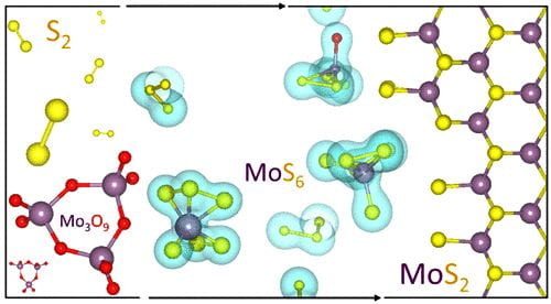
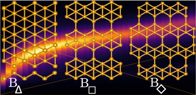
Rice materials theorist Boris Yakobson, graduate student Jincheng Lei and alumnus Yu Xie of Rice’s Brown School of Engineering have unveiled how a popular 2D material, molybdenum disulfide (MoS2), flashes into existence during chemical vapor deposition (CVD).

Knowing how the process works will give scientists and engineers a way to optimize the bulk manufacture of MoS2 and other valuable materials classed as transition metal dichalcogenides (TMDs), semiconducting crystals that are good bets to find a home in next-generation electronics.

Their study in the American Chemical Society journal ACS Nano focuses on MoS2‘s “pre-history”, specifically what happens in a CVD furnace once all the solid ingredients are in place. CVD, often associated with graphene and carbon nanotubes, has been exploited to make a variety of 2D materials by providing solid precursors and catalysts that sublimate into gas and react. The chemistry dictates which molecules fall out of the gas and settle on a substrate, like copper or silicone, and assemble into a 2D crystal.

– See more at Rice News

Borophene on silver grows freely into an atomic ‘skin’

Rice scientists lead effort to improve manufacture of valuable 2D material

Borophene has a nearly perfect partner in a form of silver that could help the trendy two-dimensional material grow to unheard-of lengths.

A well-ordered lattice of silver atoms makes it possible to speed the growth of pristine borophene, the atom-thick allotrope of boron that so far can only form via synthesis by molecular-beam epitaxy (MBE).

By using a silver substrate and through careful manipulation of temperature and deposition rate, scientists have discovered they can grow elongated hexagon-shaped flakes of borophene. They suggested the use of a proper metal substrate could facilitate the growth of ultrathin, narrow borophene ribbons.

New work published in Science Advances by researchers at Rice and Northwestern universities, Nanjing University of Aeronautics and Astronautics and Argonne National Laboratory will help streamline the manufacture of the conductive material, which shows potential for use in wearable and transparent electronics, plasmonic sensors and energy storage.

– See more at Rice News

Gold soaks up boron, spits out borophene

Rice, Argonne, Northwestern scientists show unique mechanism makes valuable 2D material

In the heat of a furnace, boron atoms happily dive into a bath of gold. And when things get cool, they resurface as coveted borophene.

The discovery by scientists from Rice University, Argonne National Laboratory and Northwestern University is a step toward practical applications like wearable or transparent electronics, plasmonic sensors or energy storage for the two-dimensional material with excellent conductivity.

Teams led by Boris Yakobson at Rice, Nathan Guisinger at Argonne and Mark Hersam at Northwestern both formed the theory for and then demonstrated their novel method to grow borophene – the atom-thick form of boron – on a gold surface.

They found that with sufficient heat in a high vacuum, boron atoms streamed into the furnace sink into the gold itself. Upon cooling, the boron atoms reappear and form islands of borophene on the surface.

This is distinct from most other 2D materials made by feeding gases into a furnace. In standard chemical vapor deposition, the atoms settle onto a substrate and connect with each other. They typically don’t disappear into the substrate.

The discovery was described in a paper in the American Chemical Society journal ACS Nano.

– See more at Rice News

Step right up for bigger 2D sheets

Rice theory shows how monocrystals of hexagonal boron nitride come together

Very small steps make a big difference to researchers who want to create large wafers of two-dimensional material.

Atom-sized steps in a substrate provide the means for 2D crystals growing in a chemical vapor furnace to come together in perfect rank. Scientists have recently observed this phenomenon, and now a Rice University group has an idea why it works.

Rice materials theorist Boris Yakobson and researcher Ksenia Bets led the construction of simulations that show atom-sized steps on a growth surface, or substrate, have the remarkable ability to keep monolayer crystal islands in alignment as they grow.

If the conditions are right, the islands join into a larger crystal without the grain boundaries so characteristic of 2D materials like graphene grown via chemical vapor deposition (CVD). That preserves their electronic perfection and characteristics, which differ depending on the material.

The Rice theory appears in the American Chemical Society journal Nano Letters.

– See more at Rice News

In borophene, boundaries are no barrier

Rice, Northwestern researchers make and test atom-thick boron’s unique domainsA scanning electron microscope image (top) shows two periodic assemblies of borophene, a synthetic, two-dimensional array of boron atoms, that join at a line defect. Computational models in the middle and bottom images correspond to the regions, with 1-to-6 borophene in red and 1-to-5 in blue. Researchers at Rice and Northwestern universities determined that phases of borophene line up in such a way that the material's conductive, metallic nature is maintained. (Credit: Graphics by Luqing Wang/Rice University)

The research led by Rice materials theorist Boris Yakobson and Northwestern materials scientist Mark Hersam appears in Nature Materials.

Borophene differs from graphene and other 2D materials in an important way: It doesn’t appear in nature. When graphene was discovered, it was famously yanked from a piece of graphite with Scotch tape. But semiconducting bulk boron doesn’t have layers, so all borophene is synthetic. Also unlike graphene, in which atoms connect to form chicken wire-like hexagons, borophene forms as linked triangles. Periodically, atoms go missing from the grid and leave hexagonal vacancies. The labs investigated forms of borophene with “hollow hexagon” concentrations of one per every five triangles and one per every six in the lattice.

Yakobson and Hersam also co-authored a recent Nature Nanotechnology perspective about “the lightest 2D metal.”In that piece, the authors suggested borophene may be ideal for flexible and transparent electronic interconnects, electrodes and displays. It could also be suitable for superconducting quantum interference devices and, when stacked, for hydrogen storage and battery applications.

– See more at Rice News

Salt boosts creation of 2D materials

Rice scientists show how salt lowers reaction temperatures to make novel materials

A dash of salt can simplify the creation of two-dimensional materials, and thanks to Rice University scientists, the reason is becoming clear.

Boris Yakobson, a Rice professor of materials science and nanoengineering and of chemistry, was the go-to expert when a group of labs in Singapore, China, Japan and Taiwan used salt to make a “library” of 2D materials that combined transition metals and chalcogens. These compounds could lead to smaller and faster transistors, photovoltaics, sensors and catalysts, according to the researchers.

Through first-principles molecular dynamics simulations and accurate energy computations, Yakobson and his colleagues determined that salt reduces the temperature at which some elements interact in a chemical vapor deposition (CVD) furnace. That makes it easier to form atom-thick layers similar to graphene but with the potential to customize their chemical composition for specific layer-material and accordingly electrical, optical, catalytic and other useful properties.

The research team including Yakobson and Rice postdoctoral researcher Yu Xie and graduate student Jincheng Lei reported its results this week in Nature.

The clip shows a molecular dynamics simulation of a layer of salt and molybdenum oxide mixing together to form molybdenum oxychloride. The atoms are oxygen (red), sodium (yellow), chlorine (green), and molybdenum (purple).

– See more at Rice News

Borophene shines alone as 2-D plasmonic material

Rice University scientists calculate flat boron capable of visible plasmon emissions

Illustration by Sharmila Shirodkar.

An atom-thick film of boron could be the first pure two-dimensional material able to emit visible and near-infrared light by activating its plasmons, according to Rice University scientists. That would make the material known as borophene a candidate for plasmonic and photonic devices like biomolecule sensors, waveguides, nanoscale light harvesters and nanoantennas. Plasmons are collective excitations of electrons that flow across the surface of metals when triggered by an input of energy, like laser light. Significantly, delivering light to a plasmonic material in one color (determined by the light’s frequency) can prompt the emission of light in another color.

Models by Rice theoretical physicist Boris Yakobson and his colleagues predict that borophene would be the first known 2-D material to do so naturally, without modification. The lab’s simulations are detailed in a paper by Yakobson with lead authors Yuefei Huang, a graduate student, and Sharmila Shirodkar, a postdoctoral researcher, in the Journal of the American Chemical Society.

– See more at Rice News

2D Boron on the Cover of Chem Soc Rev

Chemical Society Reviews features our review on two-dimensional boron on its front cover

In a recent article, we review the current theoretical and experimental progress in realizing boron atomic layers. Starting by describing a decade-long effort towards understanding the size-dependent structures of boron clusters, we present how theory plays a role in extrapolating boron clusters into 2D form, from a freestanding state to that on substrates, as well as in exploring practical routes for their synthesis that recently culminated in experimental realization. While 2D boron has been revealed to have unusual mechanical, electronic and chemical properties, materializing its potential in practical applications remains largely impeded by lack of routes towards transfer from substrates and controlled synthesis of quality samples.

The review is on the list of referee-recommended articles, HOT Chem Soc Rev articles for October, and is free to access until 13th December 2017.

New Wave of 2D Boron

Rice University researchers say 2-D boron may be best for flexible electronics

2d-b-wave
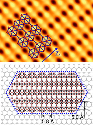
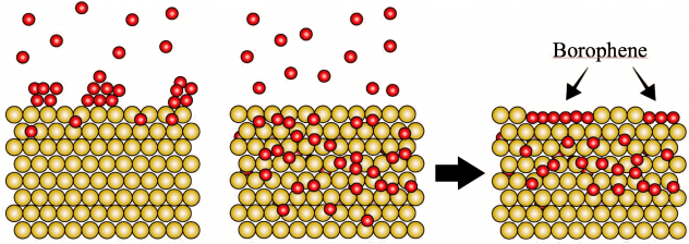
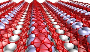
Though they’re touted as ideal for electronics, two-dimensional materials like graphene may be too flat and hard to stretch to serve in flexible, wearable devices. “Wavy” borophene might be better, according to Rice University scientists.

The Rice lab of theoretical physicist Boris Yakobson and experimental collaborators observed examples of naturally undulating, metallic borophene, an atom-thick layer of boron, and suggested that transferring it onto an elastic surface would preserve the material’s stretchability along with its useful electronic properties.

Highly conductive graphene has promise for flexible electronics, Yakobson said, but it is too stiff for devices that also need to stretch, compress or even twist. But borophene deposited on a silver substrate develops nanoscale corrugations. Weakly bound to the silver, it could be moved to a flexible surface for use.

The research appears this month in the American Chemical Society journal Nano Letters.

In The News

Polyphony in B flat

At last, experiments offer two-dimensional boron… on a silver platterb_cards

In an extensive “News & Views” in Nature Chemistry, we provide a critical view of the latest breakthrough in materials flatland: the synthesis of two-dimensional boron. It also reflects on a decade-long effort in Yakobson’s group towards understanding and eventually predicting the structure of low-dimensional boron: from the B80 fullerene, to the polymorphism of 2D boron, to practical routes for its synthesis.

2D Boron among the Angew. Chem. covers

angew_chem_cover

Two-dimensional boron would take different forms, depending on the substrate used in chemical vapor deposition growth. Image by Zhuzha Zhang

Our most recent work on 2D boron will be featured on a cover of the upcoming issue of Angewandte Chemie International Edition. The study builds on two of our previous works on two-dimensional boron  and provides further clues as to how this elusive material can be synthesized and what the product may look like.

Calculation of the atom-by-atom energies involved in creating a sheet of boron revealed that the metal substrate – the surface upon which two-dimensional materials are grown in a chemical vapor deposition (CVD) furnace – would make all the difference.

The new calculations show it may be possible to guide the formation of 2D boron by tailoring boron-metal interactions.Theoretical physicist Boris Yakobson and his Rice colleagues discovered that copper, a common substrate in graphene growth, might be best to obtain flat boron, while other metals would guide the resulting material in their unique ways.

1.
Penev, E. S., Bhowmick, S., Sadrzadeh, A. & Yakobson, B. I. Polymorphism of Two-Dimensional Boron. Nano Lett. 12, 2441–2445 (2012).
1.
Liu, Y., Penev, E. S. & Yakobson, B. I. Probing the Synthesis of Two-Dimensional Boron by First-Principles Computations. Angew. Chem. Int. Ed. 52, 3156–3159 (2013).

– See more at: Rice News