Rice lab peers inside 2D crystal synthesis

Simulations could help molecular engineers enhance creation of semiconducting nanomaterials

Scientific studies describing the most basic processes often have the greatest impact in the long run. A new work by Rice University engineers could be one such, and it’s a gas, gas, gas for nanomaterials.

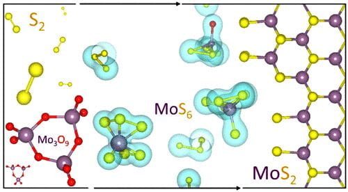
Rice materials theorist Boris Yakobson, graduate student Jincheng Lei and alumnus Yu Xie of Rice’s Brown School of Engineering have unveiled how a popular 2D material, molybdenum disulfide (MoS2), flashes into existence during chemical vapor deposition (CVD).

Knowing how the process works will give scientists and engineers a way to optimize the bulk manufacture of MoS2 and other valuable materials classed as transition metal dichalcogenides (TMDs), semiconducting crystals that are good bets to find a home in next-generation electronics.

Their study in the American Chemical Society journal ACS Nano focuses on MoS2‘s “pre-history”, specifically what happens in a CVD furnace once all the solid ingredients are in place. CVD, often associated with graphene and carbon nanotubes, has been exploited to make a variety of 2D materials by providing solid precursors and catalysts that sublimate into gas and react. The chemistry dictates which molecules fall out of the gas and settle on a substrate, like copper or silicone, and assemble into a 2D crystal.

– See more at Rice News

2D coplanar heterojunctions on the cover of J. Phys. Chem. Lett.

Our work on dimensionality-reduced Fermi level pinning in coplanar 2D heterojunctions is featured in the May issue of J. Phys. Chem. Lett. 

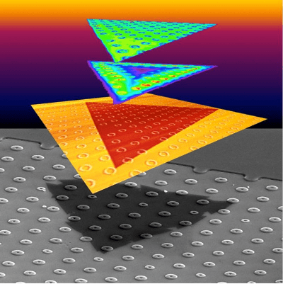
Electronic transport through a metal | semiconductor (M|S) heterojunction is largely determined by its Schottky barrier.  In light of the general interest in building 2D electronics, in a just-published work in J. Phys. Chem. Lett. we discover the relevant material parameters which dictate the behavior and strength of Fermi level pinning in 2D M|S contacts, using a multiscale model combining first-principles, continuum electrostatics, and transport calculations.

The cover is a graphical representation of the Fermi level pinning in 2D coplanar M|S  contacts which is greatly reduced due to weak electric screening in low dimensions. The interface states, while unable to alter the band alignment as in 3D, create a thin “spire” barrier to the transport electrons. Hence, the pinning strength in 2D contacts is now controlled by a new parameter: the interface width. These findings should guide the methods of contact engineering for future 2D electronic devices.

2D-materials prediction is on the Cover of ACS Nano

ACS Nano features our review on theoretical prediction of two-dimensional materials, behavior, and properties on its April front cover

Predictive modeling of 2D materials is at the crossroad of two current rapidly growing interests: 2D materials per se, massively sought after and explored in experimental laboratories, and materials theoretical-computational models in general, flourishing on a fertile mix of condensed-matter physics and chemistry with advancing computational technology. In the April issue of ACS Nano we briefly overview the general methods and specific techniques of modeling, along with a somewhat philosophical assessment of what “prediction” is, followed by selected practical examples for 2D materials, from structures and properties, to device functionalities and synthetic routes for their making. We conclude with a brief sketch–outlook of future developments.

The cover image represents the persistence of the scientific quest for two-dimensional materials that motivates their prediction. In the extraterrestrial landscape, inspired by an iconic Salvador Dalí painting, one should wonder what magnitude of gravity g would shape the graphene flake this way? Theory can predict, from first principles.

Nicholas Tjahjono awarded NASA space tech research fellowship

Rice PhD student aims to aid in NASA’s Artemis mission to the moon and beyond

Nicholas Tjahjono, a first-year doctoral student in Yakobson Research Group,  has been awarded the NASA Space Technology Graduate Research Opportunities Fellowship.

His research proposal, “Virtual Prototyping of Multifunctional Boron-Nitrogen Nanostructures and their Composites for Extreme Space Environments,” aims to aid in NASA’s Artemis mission to the moon and beyond.

The goal of Artemis is to land two astronauts on the moon by 2024 and explore the feasibility of establishing sustainable colonies, in preparation for sending the first astronauts to Mars by 2030. Tjahjono’s objective is to develop materials capable of operating under, and protecting astronauts from, extreme space environments such as extreme heat and cold, variable gravity, abrasive lunar dust, galactic cosmic radiation and solar particle events.

Nicholas earned his B.S. in the joint major of bioengineering and materials science and engineering, and his B.A. in music, from the University of California at Berkeley in 2018. Before coming to Rice, he worked as a research assistant in the Lawrence Berkeley National Laboratory’s Molecular Foundry in Berkeley, Calif.

‘Defective’ carbon simplifies hydrogen peroxide production

Plasma processing modifies carbon black powder to catalyze valuable chemical

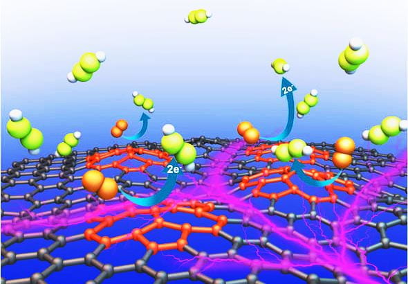
Rice University researchers have created a “defective” catalyst that simplifies the generation of hydrogen peroxide from oxygen.

Rice scientists treated metal-free carbon black, the inexpensive, powdered product of petroleum production, with oxygen plasma. The process introduces defects and oxygen-containing groups into the structure of the carbon particles, exposing more surface area for interactions.

When used as a catalyst, the defective particles known as CB-Plasma reduce oxygen to hydrogen peroxide with 100% Faradaic efficiency, a measure of charge transfer in electrochemical reactions. The process shows promise to replace the complex anthraquinone-based production method that requires expensive catalysts and generates toxic organic byproducts and large amounts of wastewater, according to the researchers.

The research by Rice chemist James Tour and materials theorist Boris Yakobson appears in the American Chemical Society journal ACS Catalysis.

– See more at Rice News

A little friction goes a long way toward stronger nanotube fibers

Rice model may lead to better materials for aerospace, automotive, medical applications

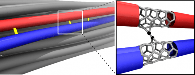
Carbon nanotube fibers are not nearly as strong as the nanotubes they contain, but Rice University researchers are working to close the gap.

A computational model by materials theorist Boris Yakobson and his team at Rice’s Brown School of Engineering establishes a universal scaling relationship between nanotube length and friction between them in a bundle, parameters that can be used to fine-tune fiber properties for strength.

The model is a tool for scientists and engineers who develop conductive fibers for aerospace, automotive, medical and textile applications like smart clothing. Carbon nanotube fibers have been considered as a possible basis for a space elevator, a project Yakobson has studied.

The research is detailed in the American Chemical Society journal ACS Nano.

– See more at Rice News

2D compound shows unique versatility

Multifunctional nanomaterial proposed by Rice could enhance solar energy, quantum computing

An atypical two-dimensional sandwich has the tasty part on the outside for scientists and engineers developing multifunctional nanodevices.

An atom-thin layer of semiconductor antimony paired with ferroelectric indium selenide would display unique properties depending on the side and polarization by an external electric field.

The field could be used to stabilize indium selenide’s polarization, a long-sought property that tends to be wrecked by internal fields in materials like perovskites but would be highly useful for solar energy applications.

Calculations by Rice materials theorist Boris Yakobson, lead author and researcher Jun-Jie Zhang and graduate student Dongyang Zhu shows switching the material’s polarization with an external electric field makes it either a simple insulator with a band gap suitable for visible light absorption or a topological insulator, a material that only conducts electrons along its surface.

Turning the field inward would make the material good for solar panels. Turning it outward could make it useful as a spintronic device for quantum computing.

The lab’s study appears in the American Chemical Society journal Nano Letters.

– See more at Rice News

CNT-graphene-borophene specialty cake

A sweet way to say “Happy Holidays”

Not everyone can make cakes, but a great cake can come from anyone… or so it seems. Combining many years of experience in modeling the synthesis of carbon nanotubes (CNTs) and 2D materials, and obviously some serious culinary skills Ksenia Bets has scaled-up their production to say “Happy Holidays” on behalf of Yakobson’s group and the MSNE department.

The cake blends a candy nanotube (CNT), graphene and borophene from sugar (or possibly other solid sources) on a stepped glazed surface. The MSNE logo can also be seen on the top terrace.

For recipes visit this page.

Rice finds path to nanodiamond from graphene

A spot of pressure enables chemical conversion to hardened 2D material

Marrying two layers of graphene is an easy route to the blissful formation of nanoscale diamond, but sometimes thicker is better.

While it may only take a bit of heat to turn a treated bilayer of the ultrathin material into a cubic lattice of diamane, a bit of pressure in just the right place can convert few-layer graphene as well.

The otherwise chemically driven process is theoretically possible according to scientists at Rice University, who published their most recent thoughts on making high-quality diamane — the 2D form of diamond — in the journal Small (featured on the inside Front Cover).

The research led by materials theorist Boris Yakobson and his colleagues at Rice’s Brown School of Engineering suggests a pinpoint of pressure on few-layer graphene, the atom-thin form of carbon known for its astonishing strength, can nucleate a surface chemical reaction with hydrogen or fluorine.

– See more at Rice News

Sunny Gupta wins Best Oral Presentation Award

Sunny Gupta, a fourth-year graduate student in Yakobson’s Group, has received a “Best Oral Presentation” Award at the 6th Annual SCI Summer Research Colloquium.

The nine judges who have listened in to all the talks were very impressed by the overall level of the presentations. They have recognized the outstanding quality of Sunny’s talk, and have assigned you one of the four SCI Bronze Oral Presentation Awards.

Sunny’s presentation covered his recent work on heterobilayers of 2D materials as a platform for excitonic superfluidity. After screening hundreds of 2D materials, a number of candidates were identified where spontaneous excitonic condensation mediated by purely electronic interaction should occur, and hetero-pairs Sb2Te2Se/BiTeCl, Hf2N2I2/Zr2N2Cl2, and LiAlTe2/BiTeI emerge promising. The predicted materials can be used to access different parts of electron-hole phase diagram, including BEC-BCS crossover, enabling tantalizing applications in superfluid transport, Josephson-like tunneling, and dissipationless charge counterflow.

– See more at Rice News

Excitons form superfluid in certain 2D combos

Rice researchers find ‘paradox’ in ground-state bilayers

Mixing and matching computational models of 2D materials led scientists at Rice University to the realization that excitons — quasiparticles that exist when electrons and holes briefly bind — can be manipulated in new and useful ways.

The researchers identified a small set of 2D compounds with similar atomic lattice dimensions that, when placed together, would allow excitons to form spontaneously. Generally, excitons happen when energy from light or electricity boosts electrons and holes into a higher state.

But in a few of the combinations predicted by Rice materials theorist Boris Yakobson and his team, excitons were observed stabilizing at the materials’ ground state. According to their determination, these excitons at their lowest energy state could condense into a superfluid-like phase. The discovery shows promise for electronic, spintronic and quantum computing applications.

The open-access study by Yakobson, graduate student Sunny Gupta and research scientist Alex Kutana, all of Rice’s Brown School of Engineering, appears in Nature Communications.

– See more at Rice News

“I do,” just in time: Newlywed grad students rush to return to Rice from India

Between an international pandemic and a dissertation defense from home, it’s a honeymoon they’ll never forget

Nitant is a Rice graduate student working in the lab of Boris Yakobson, while Lehigh University grad student Megha is preparing to defend her dissertation.

Their honeymoon was unique. Now, as the newlyweds adhere to social distancing guidelines put in place to combat the coronavirus pandemic, Nitant Gupta and Megha Sharma Gupta are spending plenty of quality time together at their new apartment in Houston.

“I am sure that Megha and I will cherish this for a long time,” Nitant said.

On March 11, the couple were married in Megha’s hometown of Udaipur, a joyous and well-attended occasion in one of India’s most beautiful cities. They were scheduled to return to the U.S. later in the month.

But with coronavirus spreading across the globe, the two graduate students quickly realized if they didn’t leave soon they might not be able to get back to Rice, where Nitant is pursuing his Ph.D. in material science.

– See more at Rice News

Double-walled nanotubes have electro-optical advantages

Rice University calculations show they could be highly useful for solar panels

One nanotube could be great for electronics applications, but there’s new evidence that two could be tops.

Rice University engineers already knew that size matters when using single-walled carbon nanotubes for their electrical properties. But until now, nobody had studied how electrons act when confronted with the Russian doll-like structure of multiwalled tubes.

The Rice lab of materials theorist Boris Yakobson has now calculated the impact of curvature of semiconducting double-wall carbon nanotubes on their flexoelectric voltage, a measure of electrical imbalance between the nanotube’s inner and outer walls.

This affects how suitable nested nanotube pairs may be for nanoelectronics applications, especially photovoltaics.

The theoretical research by Yakobson’s Brown School of Engineering group appears in the American Chemical Society journal Nano Letters.

– See more at Rice News

A small step for atoms, a giant leap for microelectronics

Nature paper reports making and moving large-scale hexagonal boron nitride

Step by step, scientists are figuring out new ways to extend Moore’s Law. The latest reveals a path toward integrated circuits with two-dimensional transistors.

A Rice University scientist and his collaborators in Taiwan and China reported in Nature today that they have successfully grown atom-thick sheets of hexagonal boron nitride (hBN) as two-inch diameter crystals across a wafer.

Surprisingly, they achieved the long-sought goal of making perfectly ordered crystals of hBN, a wide band gap semiconductor, by taking advantage of disorder among the meandering steps on a copper substrate. The random steps keep the hBN in line.

Brown School of Engineering materials theorist Boris Yakobson is co-lead scientist on the study with Lain-Jong (Lance) Li of the Taiwan Semiconductor Manufacturing Co. (TSMC) and his team. Yakobson and Chih-Piao Chuu of TSMC performed theoretical analysis and first principles calculations to unravel the mechanisms of what their co-authors saw in experiments.

– See more at Rice News

Stretched to the Limit and Sparkling on Curved Surfaces

Department of Energy’s Office of Science (BES) highlights our work with ORNL

Image courtesy of Oak Ridge National Laboratory

… Scientists use chemical vapor deposition to deposit WS2 films on substrates that have first been lithographically patterned with three-dimensional features such as trenches and tori (donut shapes).

The team has developed a model that explains that the accelerated crystal growth caused by the strain is because of an increase in the number of sites at which new particles are deposited during film growth (nucleation). When the height of the donut or trench is too high (above 40 nm), the strain becomes too high, and the films crack to release the strain.

– See more at energy.gov

Related: