
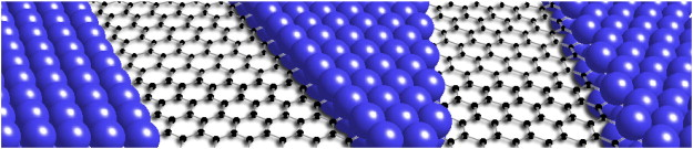
Rice theorists find mechanism behind nearly pure nanotubes from the unusual catalyst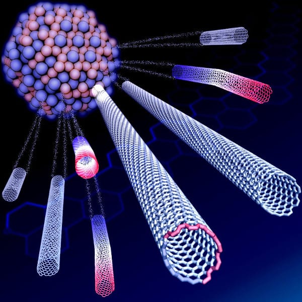
Growing a batch of carbon nanotubes that are all the same may not be as simple as researchers had hoped, according to Rice University scientists.
Rice materials theorist Boris Yakobson and his team bucked a theory that when growing nanotubes in a furnace, a catalyst with a specific atomic arrangement and symmetry would reliably make carbon nanotubes of like chirality, the angle of its carbon-atom lattice.
Instead, they found the catalyst in question starts nanotubes with a variety of chiral angles but redirects almost all of them toward a fast-growing variant known as (12,6). The cause appears to be a Janus-like interface that is composed of armchair and zigzag segments – and ultimately changes how nanotubes grow.
The Rice theoretical study detailed in the American Chemical Society journal Nano Letters could be a step toward catalysts that produce homogeneous batches of nanotubes, Yakobson said.
– See more at Rice News


