Graphene nano-coils are natural electromagnets

Rice University researchers discover graphene spirals could challenge macro solenoids
nanosol

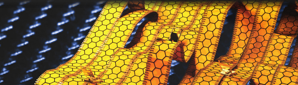
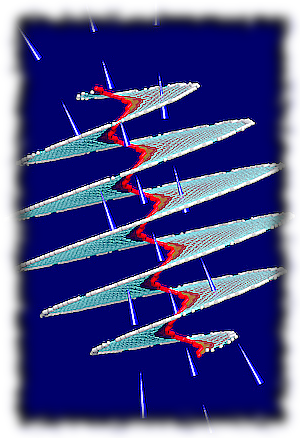
A nano-coil made of graphene could be an effective solenoid inductor for electronic applications.

In the drive to miniaturize electronics, solenoids have become way too big, say Rice University scientists who discovered, in an article just published by Nano Lett., the essential component can be scaled down to nano-size with macro-scale performance.

The secret is in a spiral form of atom-thin graphene that, remarkably, can be found in nature, according to Rice theoretical physicist Boris Yakobson and his colleagues.

“Usually, we determine the characteristics for materials we think might be possible to make, but this time we’re looking at a configuration that already exists,” Yakobson said. “These spirals, or screw dislocations, form naturally in graphite during its growth, even in common coal.”

– See more at: Rice News

2D Boron among the Angew. Chem. covers

angew_chem_cover

Two-dimensional boron would take different forms, depending on the substrate used in chemical vapor deposition growth. Image by Zhuzha Zhang

Our most recent work on 2D boron will be featured on a cover of the upcoming issue of Angewandte Chemie International Edition. The study builds on two of our previous works on two-dimensional boron  and provides further clues as to how this elusive material can be synthesized and what the product may look like.

Calculation of the atom-by-atom energies involved in creating a sheet of boron revealed that the metal substrate – the surface upon which two-dimensional materials are grown in a chemical vapor deposition (CVD) furnace – would make all the difference.

The new calculations show it may be possible to guide the formation of 2D boron by tailoring boron-metal interactions.Theoretical physicist Boris Yakobson and his Rice colleagues discovered that copper, a common substrate in graphene growth, might be best to obtain flat boron, while other metals would guide the resulting material in their unique ways.

1.
Penev, E. S., Bhowmick, S., Sadrzadeh, A. & Yakobson, B. I. Polymorphism of Two-Dimensional Boron. Nano Lett. 12, 2441–2445 (2012).
1.
Liu, Y., Penev, E. S. & Yakobson, B. I. Probing the Synthesis of Two-Dimensional Boron by First-Principles Computations. Angew. Chem. Int. Ed. 52, 3156–3159 (2013).

– See more at: Rice News

“Why nanotubes grow chiral” earns a spot in C&EN Nanotube hiStory

cq5dam.web.260.10000

JUNE 8, 2015 ISSUE, VOL. 93 | ISS. 23 Twists And Shouts: A Nanotube Story Nanotechnology’s chiral superstars were overshadowed by hype, but researchers believe they still have potential

The June 8 issue of the American Chemical Society‘s C&EN magazine quotes Boris Yakobson in its Cover Story “Twists And Shouts: A Nanotube Story“.

The timeline of major events in the history of carbon nanotubes features the Artyukhov–Penev–Yakobson (APY) theory of nanotube chirality in the most recent “Nanotubes Today” chapter. The APY theory combines the nanotube/catalyst interface thermodynamics with the kinetic growth theory to show that the unusual near-armchair peaks, repeatedly revealed in catalytic growth experiments over the last decade, emerge from the two antagonistic trends at the interface: energetic preference towards achiral versus the faster growth kinetics of chiral nanotubes. This narrow distribution is inherently related to the peaked behaviour of a simple function, xe−x.

1.
Artyukhov, V. I., Penev, E. S. & Yakobson, B. I. Why nanotubes grow chiral. Nat Commun 5, (2014).

Symmetry matters in graphene growth

Rice researchers find subtle interactions with substrate may lead to better control 

Graphene islands formed in two distinctly different shapes on separate grains of copper (colored in blue and red) grown simultaneously because the substrates' atomic lattices have different orientations, according to Rice University researchers. Image by Y. Hao/coloring by V. Artyukhov

What lies beneath growing islands of graphene is important to its properties, according to a new study led by Rice University.

Scientists at Rice analyzed patterns of graphene – a single-atom-thick sheet of carbon – grown in a furnace via chemical vapor deposition. They discovered that the geometric relationship between graphene and the substrate, the underlying material on which carbon assembles atom by atom, determines how the island shapes emerge. The study led by Rice theoretical physicist Boris Yakobson and postdoctoral researcher Vasilii Artyukhov shows how the crystalline arrangement of atoms in substrates commonly used in graphene growth, such as nickel or copper, controls how islands form. The results appear this week in Physical Review Letters.

– See more at: Rice News

Editor’s Highlights for Carbon selects our work on fibers

A recent work from the group on atomistic modeling of carbon fibers appears in the quarterly Editor’s Highlights for Carbon. These articles are handpicked by the Editors for the reader community and are made freely available for a limited time.

Carbon fiber structure is excessively complex and modeling attempts necessarily rely on various approximations. We have designed structural faults with atomistic details, pertaining to polyacrylonitrile (PAN) derived fibers, and probed them using large-scale molecular dynamics simulations to uncover trends and gain insight into the effect of local structure on the strength of the basic structural units (BSUs) and the role of interfaces between regions with different degrees of graphitization. Besides capturing the expected strength degrading with increasing misalignment, the designed basic structural units reveal atomistic details of local structural failure upon tensile loading.

The image shows an atomistic representation of a BSU (~ 40,000 atoms); for clarity part of the geometry is not rendered. A misoriented block  is highlighted. Load is applied along the fiber axis, as indicated by the thick arrow, by displacing thin slabs (“handles”) at the top and bottom of the system, schematically represented as plates.

The latest fashion: Graphene edges can be tailor-made

Rice University theory shows it should be possible to tune material’s properties

Graphene nanoribbons can be enticed to form favorable "reconstructed" edges by pulling them apart with the right force and at the right temperature, according to researchers at Rice University. The illustration shows the crack at the edge that begins the formation of five- and seven-atom pair under the right conditions. Illustration by ZiAng Zhang

Theoretical physicists at Rice University are living on the edge as they study the astounding properties of graphene. In a new study, they figure out how researchers can fracture graphene nanoribbons to get the edges they need for applications.

New research by Rice physicist Boris Yakobson and his colleagues shows it should be possible to control the edge properties of graphene nanoribbons by controlling the conditions under which the nanoribbons are pulled apart.

In the work, which appeared this month in the Royal Society of Chemistry journal Nanoscale, the Rice team used sophisticated computer modeling to show it’s possible to rip nanoribbons and get graphene with either pristine zigzag edges or what are called reconstructed zigzags.

– See more at: Rice News

Sinuous grain boundaries in graphene demystified

The January 21 issue of Adv. Funct. Mater. features on its back cover work on graphene grain boundaries

The image shows a simulated grain boundary stitching two graphene domains tilted at a 28° angle exhibits a well-defined sinuous shape, which is revealed to be energetically preferred. Such sinuous grain boundary, appeared to be a curved river on land, are highlighted by B. I. Yakobson and co-workers on page 367 as a new channel to explore novel electronic behavior in graphene and to reach the as yet unexplored flatlands of two-dimensional materials.

Sparking Industrial Breakthroughs

2015 CASC Brochure features work from the group

Images illustrating two works from the group are featured in the 2015 Brochure published by the Coalition for Academic Scientific Computation – an alliance of 79 of America’s most forward thinking research universities, national labs and computing centers, including Rice’s Ken Kennedy Institute for Information Technology.  On page 2, the  highlight box “Something new under the sun” shows a collage based on a recent Nanoscale paper, and our extensive sampling of the CNT end-caps energy landscape, published in ACS Nano, is featured in the top box on page 3.


Study of Li nucleation on graphene earns “Best Poster” Nomination

Mingjie Liu, a graduate student in Yakobson’s Group, has been named as a “Best Poster” nominee at the 2014 MRS Fall Meeting

The poster presents a recent work on the Li clustering process on graphene, reporting the geometries, nucleation barriers and electronic structure of the clusters using first principles calculations. The concentration-dependent nucleation barrier for Li on graphene was estimated as well. While the nucleation occurs more readily with increasing Li concentration, potentially leading to the dendrite formation and failure of the Li-ion battery, the existence of the barrier delays nucleation and may allow Li storage on graphene. The electronic structure and charge transfer analyses reveal how the fully-ionized Li adatoms transform to metallic Li during the cluster growth on graphene.

As a reward, nominees are offered the opportunity to record a short talk about their posters which will then be posted to MRS OnDemand®.

2D Phosphorus on the cover of Nano Letters

Nano Letters features our work on the cover of its December 2014 issue

In a recent Nano Lett. article, we demonstrate that a 2D mono-elemental semiconductor is a promising candidate. This is exemplified by first-principles study of 2D phosphorus (P), a recently fabricated high-mobility semiconductor. Most of the defects, including intrinsic point defects and grain boundaries, are electronically inactive, thanks to the homoelemental bonding, which is not preferred in heteroelemental system such as MX2. Unlike MX2, the edges of which create deep gap states and cannot be eliminated by passivation, the edge states of 2D P can be removed from the band gap by hydrogen termination. We further find that both the type and the concentration of charge carriers in 2D P can be tuned by doping with foreign atoms.

The cover image represents a “phosphorescent” rendering of some structural and electronic signatures of 2D phosphorus arranged in a collage inspired by the digital rain from “The Matrix” movie.

See more at: Rice News: Phosphorus ‘rain’

Why do nanotubes grow chiral?

Rice University theorists determine factors that give tubes their chiral angles

Many a great idea springs from talks over a cup of coffee. But it’s rare and wonderful when a revelation comes from the cup itself.

Rice University theoretical physicist Boris Yakobson, acting upon sudden inspiration at a meeting last year in Arlington, Va., obtained a couple of spare coffee cups from a server and a pair of scissors and proceeded to lay out – science fair-style – an idea that could have far-reaching implications for the nanotechnology industry.

As reflected in a new paper in Nature Communications, Yakobson and his Rice colleagues, postdoctoral researcher Vasilii Artyukhov and research scientist Evgeni Penev, had come up with the seed (or perhaps, bean) of a simple formula that describes why nanotubes have chirality. Chirality is the property that describes the angle of the carbon atom hexagons that make up a nanotube’s walls.

– See more at: Rice News

Phosphorus a promising semiconductor

Rice University physicists find 2-D form pays no heed to defects

Defects damage the ideal properties of many two-dimensional materials, like carbon-based graphene. Phosphorus just shrugs.

That makes it a promising candidate for nano-electronic applications that require stable properties, according to new research by Rice University theoretical physicist Boris Yakobson and his colleagues.

In a paper in the American Chemical Society journal Nano Letters, the Rice team analyzed the properties of elemental bonds between semiconducting phosphorus atoms in 2-D sheets. Two-dimensional phosphorus is not theoretical; it was recently created through exfoliation from black phosphorus.

– See more at: Rice News

Carbyne morphs when stretched

Rice University calculations show carbon-atom chain would go metal to semiconductor

Applying just the right amount of tension to a chain of carbon atoms can turn it from a metallic conductor to an insulator, according to Rice University scientists.

Stretching the material known as carbyne — a hard-to-make, one-dimensional chain of carbon atoms — by just 3 percent can begin to change its properties in ways that engineers might find useful for mechanically activated nanoscale electronics and optics.

The finding by Rice theoretical physicist Boris Yakobson and his colleagues appears in the American Chemical Society journal Nano Letters.

– See more at: Rice News

Caps not the culprit in nanotube chirality

Rice study narrows the possibilities for gaining control of nanotube type

A single-walled carbon nanotube grows from the round cap down, so it’s logical to think the cap’s formation determines what follows. But according to researchers at Rice University, that’s not entirely so.

Theoretical physicist Boris Yakobson and his Rice colleagues found through exhaustive analysis that those who wish to control the chirality of nanotubes – the characteristic that determines their electrical properties – would be wise to look at other aspects of their growth.

In the study by Yakobson, research scientist Evgeni Penev and postdoctoral researcher Vasilli Artyukhov that was published recently by the American Chemical Society journal ACS Nano, the Rice researchers found that the elastic energy landscapes involved in cap formation are not strong enough to dictate the nanotube’s chirality….more