New Wave of 2D Boron

Rice University researchers say 2-D boron may be best for flexible electronics

2d-b-wave
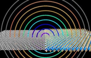
Though they’re touted as ideal for electronics, two-dimensional materials like graphene may be too flat and hard to stretch to serve in flexible, wearable devices. “Wavy” borophene might be better, according to Rice University scientists.

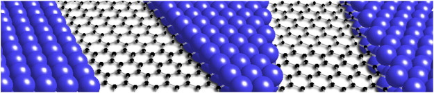
The Rice lab of theoretical physicist Boris Yakobson and experimental collaborators observed examples of naturally undulating, metallic borophene, an atom-thick layer of boron, and suggested that transferring it onto an elastic surface would preserve the material’s stretchability along with its useful electronic properties.

Highly conductive graphene has promise for flexible electronics, Yakobson said, but it is too stiff for devices that also need to stretch, compress or even twist. But borophene deposited on a silver substrate develops nanoscale corrugations. Weakly bound to the silver, it could be moved to a flexible surface for use.

The research appears this month in the American Chemical Society journal Nano Letters.

In The News

Ultra-flat circuits will have unique properties

Rice University lab studies 2-D hybrids to see how they differ from common electronics

The old rules don’t necessarily apply when building electronic components out of two-dimensional materials, according to scientists at Rice University.2d-junct

The Rice lab of theoretical physicist Boris Yakobson analyzed hybrids that put 2-D materials like graphene and boron nitride side by side to see what happens at the border. They found that the electronic characteristics of such “co-planar” hybrids differ from bulkier components.

Their results appear this month in the American Chemical Society journal Nano Letters.

Shrinking electronics means shrinking their components. Academic labs and industries are studying how materials like graphene may enable the ultimate in thin devices by building all the necessary circuits into an atom-thick layer.

– See more at Rice News

Luqing Wang wins Franz and Frances Brotzen Fellowship Award

Luqing Wang, a third-year graduate student in Yakobson’s Group, has received the 2016 Franz and Frances Brotzen Fellowship Award from the MSNELuqing Department. To honor Franz R. Brotzen, the Stanley C. Moore Professor Emeritus of Materials Science and a former dean of engineering, this fellowship was established by David Lee Davidson and his wife, Patricia, and to support an endowed fellowship for graduate students researching in the area of materials science.

Luqing’s research focuses on predicting novel properties and understanding the cutting-edge mechanism of new two-dimensional materials based on  first-principles calculations. She explores many-body and spin-orbit effects on the electronic structure of strained monolayer transition metal dichalcogenides, and the enhanced electro-mechanical anisotropy of phosphorene caused by the effects of uniaxial stress along an arbitrary direction. She also works on morphologies and phase transitions in tin sulfides, as well as routes for their controlled synthesis.

Polyphony in B flat

At last, experiments offer two-dimensional boron… on a silver platterb_cards

In an extensive “News & Views” in Nature Chemistry, we provide a critical view of the latest breakthrough in materials flatland: the synthesis of two-dimensional boron. It also reflects on a decade-long effort in Yakobson’s group towards understanding and eventually predicting the structure of low-dimensional boron: from the B80 fullerene, to the polymorphism of 2D boron, to practical routes for its synthesis.

Yakobson Group at the Spring ’16 Faculty Data Science Meetup

Check out our posters at the Spring ’16 Faculty Data Science Meetup hosted by the poster_tinyKen Kennedy Institute for Information Technology (April 13, 2016, 3-5pm, BioScience Research Collaborative Building (BRC) Event/Exhibit Hall):

Digging into Big Data of 2D nanomaterials… for fun and profit

Steady progress in computing power has motivated computational materials scientists to try new approaches to modeling materials. Here we explore data-driven and data-centric approaches to explain the properties and behavior of real advanced materials or accelerate the discovery of new ones. Often, this necessitates the sampling of enormous configurational spaces due to chemical and/or structural variety and processing the associated `big-data’ computational output. Selected examples are presented illustrating a state-of-the-art approach that allows for an elegant use of statistical mechanics methods (“cluster expansion”) in combination with first-principles density-functional theory (DFT) calculations, leading to a thorough exploration of the configurational space.

Materials systems include the alloys of two-dimensional transition-metal dichalcogenides M1-xM’xX2yX’2(1-y), the 2D materials family within the B-N-C phase diagram, the peculiar, no longer hypothetical,  2D polymorphs of elemental boron, as well the end-caps of single walled carbon nanotubes.

Can Two-Dimensional Boron Superconduct?

Rice University scientists predict 2-D material – no longer theoretical – has unique propertiesimg4news_small

Rice University scientists have determined that two-dimensional boron is a natural low-temperature superconductor. In fact, it may be the only 2-D material with such potential.

Rice theoretical physicist Boris Yakobson and his co-workers published their calculations that show atomically flat boron is metallic and will transmit electrons with no resistance. The work appears this month in the American Chemical Society journal Nano Letters.

The hitch, as with most superconducting materials, is that it loses its resistivity only when very cold, in this case between 10 and 20 kelvins (roughly, minus-430 degrees Fahrenheit). But for making very small superconducting circuits, it might be the only game in town.

– See more at Rice News

The Carbon NanoSolenoid on the Cover of Nano Letters

Nano Letters features our work on the Cover of its January 2016 issue

nalefd_v016i001.indd
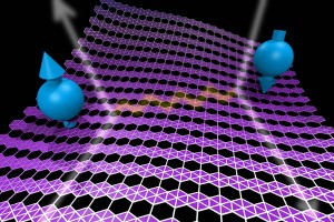
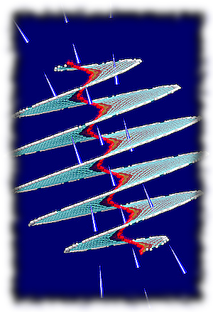
Graphene forms helicoids, akin to the mathematical Riemann surface for log(z), naturally occurring as screw dislocations in graphite or anthracite. In the Nano Letters paper, we demonstrate that the miniscule pitch of such winding carbon ribbons endows them with largest magnetic inductance per volume, which surpasses any current technologies. If voltage is applied, electrical current must flow helically, producing near the center strong magnetic field orders of magnitude greater than that of planet Earth.

The image was produced from the actual atomic geometry, using VMD, our own Edgecount tool, MeshLab, Python scripting, and the mighty Gimp.

New Materials for Better Electronics

2016 CASC Brochure features work from the group

casc2016An image illustrating recent work from the group is featured in the 2016 Brochure
published by the Coalition for Academic Scientific Computation – an alliance of 85 of America’s most forward thinking research universities, national labs and computing centers, including Rice’s Ken Kennedy Institute for Information Technology.
On page 13, the highlight box “New Materials for Better Electronics” features our recent work on two-dimensional black phosphorus.

Nano Lett. about Nano Letters

…or the indentation response of individual CNT junctions

Rice University scientists used a picoindenter to measure the stiffness of junctions in a nanotube "alphabet." They determined its letters handle strain to varying degrees depending on their form. The image shows a few carbon "nano letters" created by graduate student Yang Yang.

Rice University scientists used a picoindenter to measure the stiffness of junctions in a nanotube “alphabet.” They determined its letters handle strain to varying degrees depending on their form. The image shows a few carbon “nano letters” created by graduate student Yang Yang.

Never mind the ABCs. Rice University scientists interested in nanotubes are studying their XYΩs.

Carbon nanotubes grown in a furnace aren’t always straight. Sometimes they curve and kink, and sometimes they branch off in several directions. The Rice researchers realized they now had the tools available to examine just how tough those branches are.

They used experiments and simulations to study the stiffness of joined nanotubes and found significant differences that are defined by their forms. It turned out that some types are tougher than others, and that all may have their uses if and when nanotubes are used to build macroscale structures.

The team led by Rice materials scientist Pulickel Ajayan and theoretical physicist Boris Yakobson named their nanotubes for their shapes: I for straight nanotubes, Y for branched, X for covalently joined tubes that cross, the lambda symbol (an upside-down “V”) for nanotubes that join at any angle and the omega symbol (Ω) for noncovalent tubes that bind through van der Waals and other forces.

The study was published by the American Chemical Society’s Nano Letters.

– See more at Rice News

Graphene nano-coils are natural electromagnets

Rice University researchers discover graphene spirals could challenge macro solenoids
nanosol

A nano-coil made of graphene could be an effective solenoid inductor for electronic applications.

In the drive to miniaturize electronics, solenoids have become way too big, say Rice University scientists who discovered, in an article just published by Nano Lett., the essential component can be scaled down to nano-size with macro-scale performance.

The secret is in a spiral form of atom-thin graphene that, remarkably, can be found in nature, according to Rice theoretical physicist Boris Yakobson and his colleagues.

“Usually, we determine the characteristics for materials we think might be possible to make, but this time we’re looking at a configuration that already exists,” Yakobson said. “These spirals, or screw dislocations, form naturally in graphite during its growth, even in common coal.”

– See more at: Rice News

2D Boron among the Angew. Chem. covers

angew_chem_cover

Two-dimensional boron would take different forms, depending on the substrate used in chemical vapor deposition growth. Image by Zhuzha Zhang

Our most recent work on 2D boron will be featured on a cover of the upcoming issue of Angewandte Chemie International Edition. The study builds on two of our previous works on two-dimensional boron  and provides further clues as to how this elusive material can be synthesized and what the product may look like.

Calculation of the atom-by-atom energies involved in creating a sheet of boron revealed that the metal substrate – the surface upon which two-dimensional materials are grown in a chemical vapor deposition (CVD) furnace – would make all the difference.

The new calculations show it may be possible to guide the formation of 2D boron by tailoring boron-metal interactions.Theoretical physicist Boris Yakobson and his Rice colleagues discovered that copper, a common substrate in graphene growth, might be best to obtain flat boron, while other metals would guide the resulting material in their unique ways.

1.
Penev, E. S., Bhowmick, S., Sadrzadeh, A. & Yakobson, B. I. Polymorphism of Two-Dimensional Boron. Nano Lett. 12, 2441–2445 (2012).
1.
Liu, Y., Penev, E. S. & Yakobson, B. I. Probing the Synthesis of Two-Dimensional Boron by First-Principles Computations. Angew. Chem. Int. Ed. 52, 3156–3159 (2013).

– See more at: Rice News

“Why nanotubes grow chiral” earns a spot in C&EN Nanotube hiStory

cq5dam.web.260.10000

JUNE 8, 2015 ISSUE, VOL. 93 | ISS. 23 Twists And Shouts: A Nanotube Story Nanotechnology’s chiral superstars were overshadowed by hype, but researchers believe they still have potential

The June 8 issue of the American Chemical Society‘s C&EN magazine quotes Boris Yakobson in its Cover Story “Twists And Shouts: A Nanotube Story“.

The timeline of major events in the history of carbon nanotubes features the Artyukhov–Penev–Yakobson (APY) theory of nanotube chirality in the most recent “Nanotubes Today” chapter. The APY theory combines the nanotube/catalyst interface thermodynamics with the kinetic growth theory to show that the unusual near-armchair peaks, repeatedly revealed in catalytic growth experiments over the last decade, emerge from the two antagonistic trends at the interface: energetic preference towards achiral versus the faster growth kinetics of chiral nanotubes. This narrow distribution is inherently related to the peaked behaviour of a simple function, xe−x.

1.
Artyukhov, V. I., Penev, E. S. & Yakobson, B. I. Why nanotubes grow chiral. Nat Commun 5, (2014).

The ultimate diamond slab…

among the most cited articles in Diamond and Related Materials published since 2010
fig6-diam_reatl_mater_2010
The ultimate diamond slab: GraphAne versus graphEne” is one of the early works from the group presenting a comprehensive characterization of three carbon nanomaterials of technological interest: graphEne, graphAne, and fluorinated graphene. By means of first principles and tight-binding calculations in combination with analytical methods, we carried out detailed comparative studies of their structural, mechanical, thermal, and electronic properties. The calculated elastic properties of these materials confirmed their high mechanical stability and stiffness, which in association with their low dimensionality, translates into a large ballistic thermal conductance. Furthermore, we showed that while graphene is a zero-gap semi-metal, graphane and fluorinated graphene are wide gap semiconductors. Here we also discussed designed interfaces between these systems, and showed that their physical properties have potential applications in nanoelectronic devices.

Symmetry matters in graphene growth

Rice researchers find subtle interactions with substrate may lead to better control 

Graphene islands formed in two distinctly different shapes on separate grains of copper (colored in blue and red) grown simultaneously because the substrates' atomic lattices have different orientations, according to Rice University researchers. Image by Y. Hao/coloring by V. Artyukhov

What lies beneath growing islands of graphene is important to its properties, according to a new study led by Rice University.

Scientists at Rice analyzed patterns of graphene – a single-atom-thick sheet of carbon – grown in a furnace via chemical vapor deposition. They discovered that the geometric relationship between graphene and the substrate, the underlying material on which carbon assembles atom by atom, determines how the island shapes emerge. The study led by Rice theoretical physicist Boris Yakobson and postdoctoral researcher Vasilii Artyukhov shows how the crystalline arrangement of atoms in substrates commonly used in graphene growth, such as nickel or copper, controls how islands form. The results appear this week in Physical Review Letters.

– See more at: Rice News

Editor’s Highlights for Carbon selects our work on fibers

A recent work from the group on atomistic modeling of carbon fibers appears in the quarterly Editor’s Highlights for Carbon. These articles are handpicked by the Editors for the reader community and are made freely available for a limited time.

Carbon fiber structure is excessively complex and modeling attempts necessarily rely on various approximations. We have designed structural faults with atomistic details, pertaining to polyacrylonitrile (PAN) derived fibers, and probed them using large-scale molecular dynamics simulations to uncover trends and gain insight into the effect of local structure on the strength of the basic structural units (BSUs) and the role of interfaces between regions with different degrees of graphitization. Besides capturing the expected strength degrading with increasing misalignment, the designed basic structural units reveal atomistic details of local structural failure upon tensile loading.

The image shows an atomistic representation of a BSU (~ 40,000 atoms); for clarity part of the geometry is not rendered. A misoriented block  is highlighted. Load is applied along the fiber axis, as indicated by the thick arrow, by displacing thin slabs (“handles”) at the top and bottom of the system, schematically represented as plates.